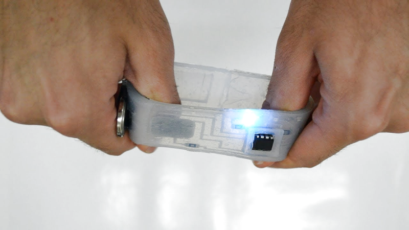
Flexible circuits built on polyimide film are now commonplace, you can prototype with them at multiple factories, at a cost that is almost acceptable to your average hacker. Polyimide film is pretty tough for something so thin, but eventually it will tear, and with larger components, bend radii are quite restricted. But what about stretchable circuits, as in circuits you can flex, twist and stretch? Let us introduce silicone devices. A research group from Hasselt University, Belgium, have been prototyping making truly flexible, silicone-based circuit substrates, managing to integrate a wide range of SMT component types with a dual layer interconnect, with vias and external contacts.
It should be possible to reproduce the process using nothing more special than your average Makerspace CO2 laser cutter, and a couple of special tools that can be easily made — a guide for that is promised — it is purely a matter of gathering a few special materials, and using off-cuts you have lying around for the rest. The interconnect uses Galinstan, which is a low melting point alloy of gallium, indium, and tin. Unfortunately, this material is fairly expensive and cannot be shipped by air due to the gallium content, without specialised handling, at considerable expense. But that aside, other than some acrylic sheets, some vinyl, copper foil and a few sprays, nothing is beyond reach.
The construction process is reverse to what we normally see, with the components and copper contact plates placed first, on to a primed vinyl sheet. This sheet is laser marked with the component outlines to enable them to be corrected placed. Yes, that’s right, they’re using a laser cutter to mark vinyl, a chlorine-containing plastic. Hold on to that thought for a bit.
Insulating layers and substrate layers are constructed by blade-coating with a layer of clear silicone. Interconnect layers are formed by sticking a fresh vinyl sheet onto the exposed contacts and laser cutting just though it to expose the pads and the interconnect traces. Next the fancy Galinstan is applied by brush and the vinyl stencil removed. Rinse and repeat for the next layer of insulating silicone, more circuit traces, then use the laser cutter to precisely etch through the via regions to allow more metalisation to be added. Finally a coating of silicone is applied over the whole assembly, the laser is again used to etch the silicone away from the contact pads, and with a little solder tinning of these, you’re done. Simple, if only our Makerspaces didn’t have rules against laser cutting vinyl.
This was clearly a very brief overview, here is a very detailed instructables guide ready for you, as well as a formal research paper, detailing why this came about and why you might want to try this yourself.
If you’re into custom wearables, you might remember this earlier piece about silicone circuits, and this one weird organic-looking thing from the same time-frame.
Thanks [Daniel] for the tip!
0 Commentaires