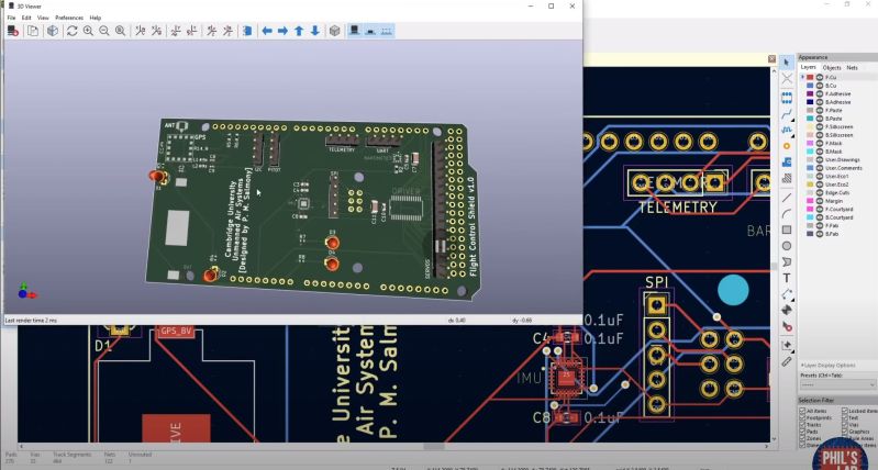
In a recent retrospective video, [Phil] from Phil’s Lab goes through a number of his early PCB designs, to critique and comment on what he likes and doesn’t like in these designs. Even though it’s only been a few a few years, he founds plenty that’s wrong. From poor and inconsistent formatting in the schematic, to sloppy and outright broken PCB layouts. It’s a fascinating look at years of lessons learned.
[Phil] comments on the importance of clear labeling and organization of sections and pages in the schematic to make it obvious what the function of a block is. Other lessons include the labeling of nets to make PCB routing a lot easier, making good use of PCB planes, getting all relevant information on components and layout in the schematic as a comment, and connecting decoupling capacitors to their relevant pins.
Although we tend to forget about older projects, it can be very interesting to take a look at them now and then, to see (hopefully) our progress over the years. In the case of [Phil] it’s fascinating to see the transition from a basic two-sided board with THT components to multi-layer boards with STM32 MCUs.
0 Commentaires