As great as cameras that operate in the visual light spectrum are, they omit a lot of the information that can be gleaned from other wavelengths. There is also the minor issue that visibility is often impacted, such as when it’s raining, or foggy. When this happens, applications such as self-driving cars which rely on this, have a major issue. Through the use of sensors that are sensitive to other wavelengths, we can however avoid many of these issues.
Short-wave infrared radiation (SWIR) is roughly the part of the electromagnetic spectrum between 1.4 μm – 3 μm, or 100 THz – 214 THz. This places it between visible light and microwaves, and above long-wave IR at 20 THz – 37 THz. LWIR is what thermal cameras use, with LWIR also emitted by warm objects, such as the human body.
SWIR is largely unaffected by water in the atmosphere, while also passing through materials that are opaque to visible light. This allowing SWIR to be used for the analysis and inspection of everything from PCBs and fruit to works of art to capture details that are otherwise invisible or very hard to see.
Unfortunately, much like thermal camera sensors, SWIR sensors are rather expensive. Or they were, until quite recently, with the emergence of quantum-dot-based sensors that significantly decrease the costs of these sensors.
Capturing Short Waves
The sensors that allows us to capture infrared radiation in general consist of a rectangular array of pixels, called a focal-plane array (FPA), also known as a staring array. This is similar to the FPAs used with other wavelengths, such as the CMOS (APS) and CCD sensors used with visible light. These FPAs are usually made of silicon, as silicon-based sensors are sensitive in the visible and part of the near-infrared spectrum.

For wavelengths beyond near infrared, more exotic materials and processes are generally required. The material for an SWIR sensor needs not only to be sensitive in that wavelength, but also to have sufficient electron mobility so that a charge can be transferred rapidly and efficiently enough to be of use in a sensor. This is where, at the moment, gallium indium arsenide (GaInAs) is most popular. (Also interchangeably referred to as InGaAs in scientific literature.)
GaInAs was first reported to have been successfully grown on an InP substrate by Duchemin et al. (1981) in 1980 using metalorganic chemical vapor deposition, which today is still the primary method of creating GaInAs sensor structures. After the vapor deposition phase, these GaInAs dies are meticulously bonded to a silicon-based interface, making it a relatively slow, labor-intensive and thus expensive process.
Which is not to say that it’s impossible to bump the price tag up even further. When the NIR sensors for the James Webb Space Telescope were developed, it was found that GaInAs sensors were too noisy and with high dark current. This led to the use of HgCdTe (mercury cadmium telluride) instead, with each sensor grown and assembled similarly to a GaInAs sensor, just with an astronomical price tag of around a quarter million US dollars each.
This points out a weakness of GaInAs-based sensors: in order to reduce the noise in the signal from thermal radiation, they are generally cooled down using a cryogenic cooler or similar solution. This adds significantly to the cost and complexity of operating these sensors.
The main take-away from this is that it demonstrates that there are multiple materials one can select and tune to a specific part of the electromagnetic spectrum. Which one works depends hereby on one’s requirements, as well as budget. As amazing as SWIR sensors would be to use with e.g. industrial production lines for QA and autonomous or driving-assisted cars to get around visual limitations in less than ideal weather, GaInAs-based sensors at thousands of dollars a piece are far too expensive to use in such applications.
The Right Trade-Offs
It would seem fairly obvious that for generic, affordable SWIR sensors we don’t need to match the exact sensitivity and speed requirements of a GaInAs-based sensor, as long as the trade-offs in terms of capture speed and sensitivity match the budgetary gains. This is why lead sulfide (PbS) based colloidal quantum dots (CQDs) have received significant attention, as these promise acceptable photosensitivity in the SWIR spectrum courtesy of the ability of QDs to be tuned rather precisely to the target spectrum.
A major issue with PbS CQDs is their long-term stabilization (passivation), with Kwon et al. (2020) reporting in Nano Convergence on the addition of cadmium sulfide (CdS) to stabilize PbS QDs for use as SWIR sensors. The resulting CQDs successfully operated for over 182 hours. The major advantage of CQDs like these over GaInAs-based sensors is that they are significantly easier and faster to synthesize, while also simplifying the integration into a functional sensor.
Instead of a vapor deposition step, the QDs are produced in a similar fashion as the QDs used in certain display technologies, with the QDs synthesized using solutions and equipment found in any well-equipped chemistry laboratory – as also described in detail by Kwon et al. – after which the resulting solution can be applied as a thin-film coating on the target substrate.
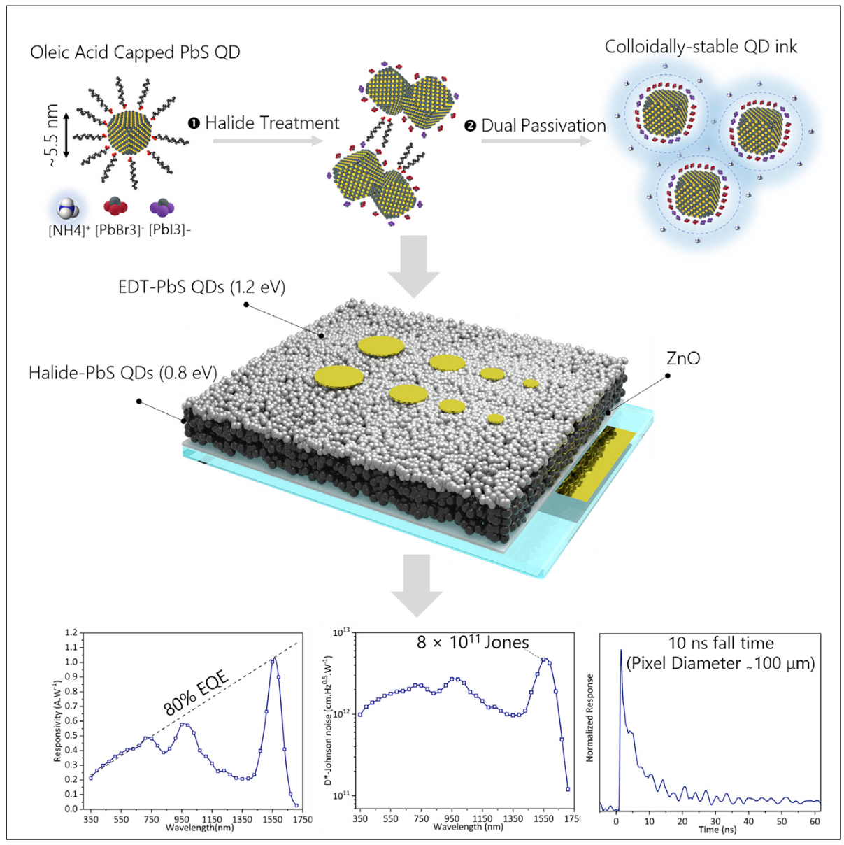
Also recently, Vafaie et al. (2020, PDF) from the University of Toronto described PbS CQDs using high-level bromine passivation, creating SWIR QDs that have not only an external quantum efficiency (EQE) of 80% at 1,550 nm (comparable to GaInAs), but also a 10 ns response time. They reported 12 hours of stable, continuous operation under ambient air.
Mind The Production Gap
Before an amazing new technology can escape from the laboratory and find its way into factories, a production process that lends itself well to mass-production has to be developed. As noted, this is where a technology like GaInAs never made it past small-scale production, but PbS CQD-based SWIR sensors appear to be doing much better.
At this point SWIR Vision Systems, Emberion, ST Microelectronics, as well as Imec have presented products using these sensors, or prototype SWIR sensors based on PbS CQDs. In January of 2022 it was announced that Hitachi Astemo as an automotive supplier will be evaluating Israeli TriEye’s Raven SWIR sensors. Being early days, it is clear that for at least a while these SWIR sensors will remain out of reach of the average hobbyist and small-scale manufacturer.
According to Imec, they expect that their SWIR sensors will ‘one day’ be manufactured for as little as €10 to €100. Compared to existing GaInAs-based solutions this would be amazing value, and put it within reach of even hobbyists once released onto the general market. This may lead one to wonder just what it is that cheap SWIR sensors would be useful for.
Inspect, Analyze, Navigate
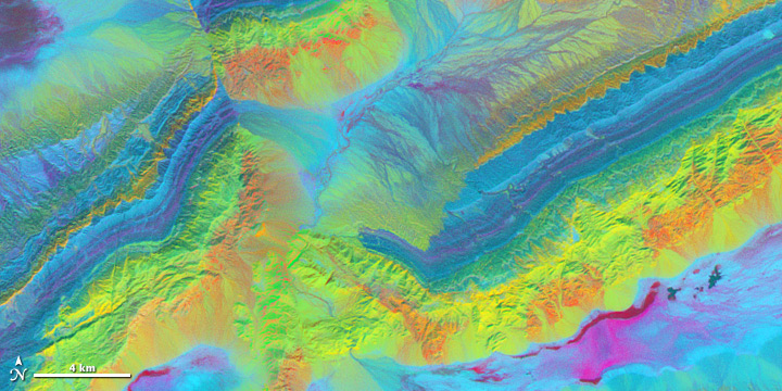
SWIR is extremely useful for contributing details that the visual part of the spectrum cannot provide, such as the mineral content in geological formations, which is essential information for NASA’s Earth Observatory project obtained using its satellites. Yet the same could be done by e.g. geologists, whether on the ground or via airplane or drone to assist surveys.
Under SWIR illumination it is also easy to see e.g. bruising in fruit, sketches hidden below the paint on a canvas, and the amount of fluid or powder left in containers that are otherwise opaque. Similarly, it is possible to see through much of PCBs and silicon, making it useful for (automated) inspections to add to existing inspection workflows.
Because SWIR is not seen by the human eye and yet reflected much like visible light, it can be used for navigation. Unlike visible light cameras, or even regular IR cameras on drones, SWIR cameras are unaffected by even the heaviest fog and rain. This is also an extremely useful property for security and wild-life cameras.
With for how many decades SWIR imaging has essentially been out of reach of the average person, it might take some time for the advantages offered to become fully obvious. Even so, when we consider the regular use that thermal cameras find today by hobbyists and professionals alike, it’s not hard to imagine SWIR cameras finding even more uses, as an alternative to both night vision (‘IR’) cameras and as an invaluable analysis tool, whether it’s sorting fruit or analyzing mineral samples.
Hopefully before long we will see CQD-based SWIR sensors become generally available. Having the current generation see use in automotive and similar markets will likely help significantly with driving down the manufacturing costs. Until then it’s still a waiting game, even as we should see these new sensors appearing in more and more devices around us.
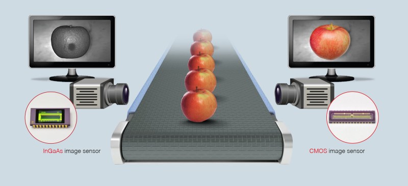
[Heading image: As apples travel down the conveyor belt, they are scanned using InGaAs and CMOS cameras. The InGaAs camera will show defects beginning to form under the skin that a human eye cannot see; the CMOS camera will show visible defects. (Credit: Hamamatsu)]


0 Commentaires