What do you get when you cross a modern super-scalar out-of-order CPU core with more traditional microcontroller aspects such as no virtual memory, no memory cache, and no DDR or PCIe controllers? You get the Tesla Dojo, which Chips and Cheese recently did a deep dive on.
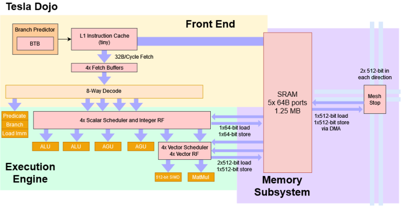
It starts with a comparison to the IBM Cell processors. The Cell of the mid-2000s featured something called the SPE (Synergistic Processing Elements). They were smaller cores focused on vector processing or other specialized types of workloads. They didn’t access the main memory and had to be given tasks by the fully featured CPU. Dojo has 1.25MB of SRAM that it can use as working memory with five ports, but it has no cache or virtual memory. It uses DMA to get the information it needs via a mesh system. The front end pulls RISC-V-like (heavily MIPS-inspired) instructions into a small instruction cache and decodes eight instructions per cycle.
Interestingly, the front end aggressively prunes instructions such as jumps or conditionals. However, eliminated instructions aren’t tracked through the pipeline. Instructions are not tracked through retirement, so during exceptions and debugging, and it’s unclear what the faulting instruction was as instructions are retired out of order.
Despite the wide front end, there are just two ALUs and two AGUs. This makes sense as the focus of integer execution is primarily focused on control flow and logic. The actual computing horsepower is the vector and matrix execution pipelines. With 512-bit vectors and 8x8x4 matrices, each dojo core comes close to a full BF26 TFLOP. The result is something that looks more like a microprocessor but is wide like a modern desktop CPU.
All these decisions might seem strange until you step back and look at what Tesla is trying to accomplish. They’re going for the smallest possible core to fit as many cores on the die as possible. Without a cache, you don’t need any snoop filters or tags in memory to maintain coherency. On TSMC’s 7nm process, the Dojo core and SRAM fit in 1.1 square millimeters. Over 71.1% of the die is spent on cores and SRAM (compared to 56% of the AMD Zeppelin). A single Dojo D1 die has 354 Dojo cores. As you can imagine, a Dojo die must communicate with an interface processor, which connects to the host computer via PCIe. However, Dojo deployments often have 25 dies, making this a very scalable supercomputer.
If you’re curious about peeling back the layers of more compute cores, look into Alder Lake.
0 Commentaires