The Serial Peripheral Interface (SPI) interface was initially standardized by Motorola in 1979 for short-distance communication in embedded systems. In its most common four-wire configuration, full-duplex data transfer is possible on the two data (MOSI, MISO) lines with data rates well exceeding 10 Mb/s. This makes SPI suitable for high-bandwidth, full-duplex applications like SD storage cards and large resolution, high-refresh displays.
STM32 devices come with a variable number of SPI peripherals, two in the F042 at 18 Mb/s and five in the F411. Across the STM32 families, the SPI peripheral is relatively similar, with fairly minor differences in the register layout. In this article we’ll look at configuring an SPI peripheral in master mode.
Defining SPI
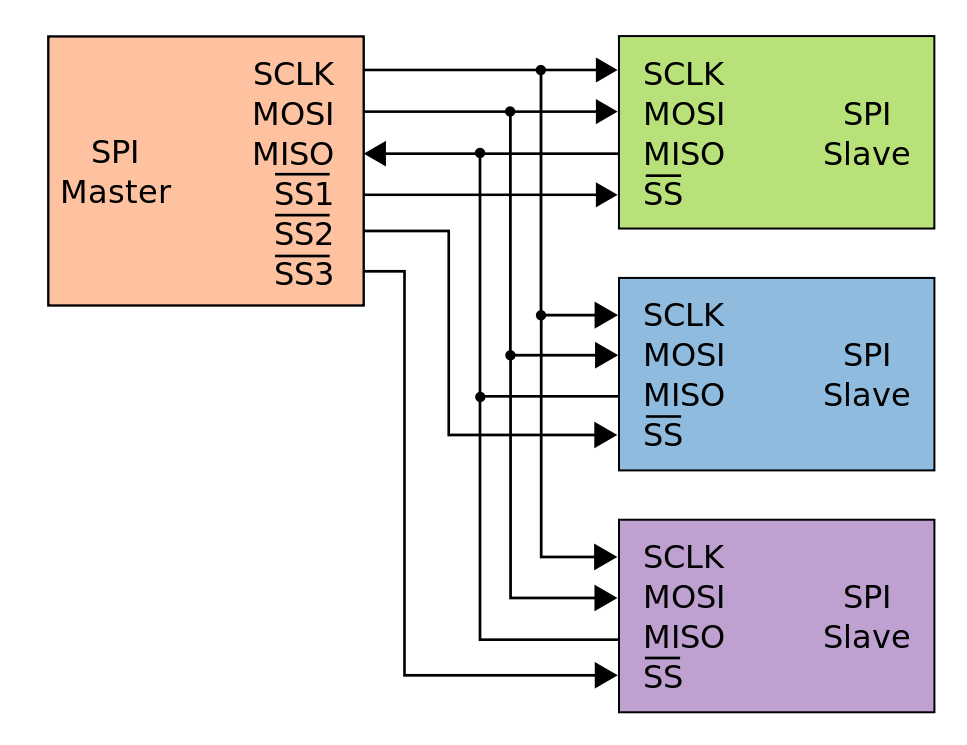
One interesting and perhaps annoying factoid with SPI is that although it can support multiple devices, it does not have an addressing bus, but instead requires that a designated pin is pulled low on the device, usually called slave select (SS) or chip select (CS). With SS high, the slave device puts its other pins into high impedance mode, effectively disconnecting from the SPI lines. The STM32 SPI peripherals have a provision for a dedicated SS pin (NSS) that can streamline this process if only one device is connected. Generally you want to use GPIO pins to toggle these SS pins, with one GPIO pin per device.
For four-wire SPI the master and slave devices are thus connected with the following lines, with the SS line duplicated for each additional slave:
- SCLK (serial clock, from master)
- MOSI (master out, slave in)
- MISO (master in, slave out)
- SS (slave select)
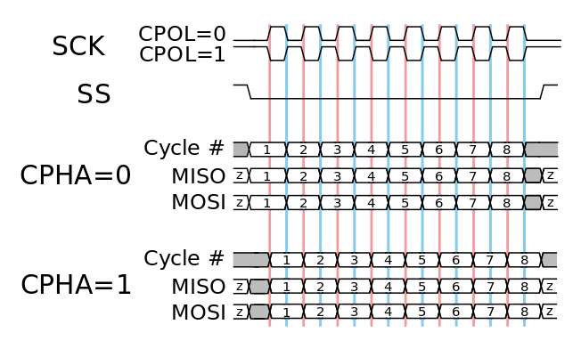
Setting up the SPI peripheral is relatively straightforward, requiring the configuration of the clock and parameters such as 8- or 16-bit transfers. Less obvious are the SPI clock polarity (CPOL) and phase (CPHA) parameters. Here the default (Mode 0) is usually CPOL 0 and CPHA 0, which translates to the clock line idling low and new data being pushed onto the data line on the trailing edge of the current clock cycle. CPOL 1 and CPHA 1 result in the opposite behavior. Slaves may support modes other than mode 0, but the datasheet for each slave has to be consulted on a case-by-case basis.
With all of this in mind, we can look at configuring SPI on both the F411 and F042 microcontrollers. Due to the aforementioned similarity between the SPI peripherals across the STM32 families it’s relatively straightforward to adapt the initialization routine. The data transfer routines themselves remain unchanged.
Setting Things Up
Setting up an SPI master begins with configuring the GPIO pins that we’ll be using. This involves setting the appropriate Alternate Function (AF) mode and pin parameters, for example AF5 on the F411 MCU’s pins 4 through 6 on port A. The SPI pins themselves are assigned the following properties:
- SCLK: floating, push-pull, high speed.
- MOSI: floating, push-pull, high speed.
- MISO: pull-up, push-pull, high speed.
- SS: pull-up, push-pull, high speed.
Since SPI relies on a push-pull configuration rather than the open-drain of I2C, we have to set all pins to match this, along with the fast GPIO speed option to keep up with the SPI signaling. The decision to leave a pin floating versus activating its pull-up is determined primarily by the function of these pins. In the case of a select pin it is essential to keep it in a high state in order to prevent accidental activation of a device before the system has finished initializing.
Activating the MISO pin’s pull-up is done to keep this line in a known state when no devices are selected and thus none of them are driving the MISO line. Even though the master is not reading the incoming data register, the intermediate voltages can potentially cause issues like excessive power draw.
With the GPIO pins thus configured, the target SPI peripheral is enabled in the relevant Reset and Clock Control (RCC) enable register. For example, the SPI 1 peripheral is enabled in the RCC_APB2ENR register, while SPI 2 and SPI 3 are generally found on the APB1 bus and thus enabled in the corresponding register in RCC. Next up is configuring the SPI peripheral itself.
The first item to configure here is the SPI clock divider (baud rate, BR) in the SPI_CR1 register. This uses the APB frequency (the peripheral bus frequency, or fPCLK) as the input for the SPI clock, which can be set to between fPCLK/2 and fPCLK/256 using three bits of resolution. The divider should be picked to achieve a reasonable clock and thus transfer speed for the application.
While on both the F0 and F4 families the default transfer size is 8-bit, the latter’s peripheral only allows for setting the data frame format to either 8- 16-bit in the SPI_CR1 DFF (Data Frame Format) register. With the F0’s SPI peripheral the range of options is far larger when configuring its DS (Data Size) value in the SPI_CR2 register. This is a 4-bit value that allows for the data size to be configured to anywhere between 4- and 16-bits, with e.g. 8-bit corresponding to b0111.
Unless there are special requirements, the default 8-bit data size, default Mode 0 configuration and default MSB-first setting are good default choices that should work with most SPI devices. This then means that only the clock divisor has to be configured in all cases, after which master mode can be enabled in SPI_CR1 (MSTR). The SS pin can then be enabled and set as output by setting SSOE in SPI_CR2.
Finally, the SPI peripheral can be enabled by setting SPE (SPI Peripheral Enable) in SPI_CR1.
Data Transfers
As mentioned earlier, SPI allows for full-duplex transfers. The complication this adds comes from the fully synchronous nature of SPI: for every byte put on the MOSI line by the master, the slave will put a byte on the MISO line, and vice versa. Since the clock line is driven by bytes sent by the master, the result is that in order to receive data from a slave, the master has to put data (e.g. null bytes) on MOSI for each byte on MISO.
A way around this is by changing the SPI bus from a four-wire to a three-wire (half-duplex) configuration using BIDIMODE in SPI_CR1, which does require cumbersome reconfiguring of the peripheral in between transfers. Generally you would want to just put null bytes on MOSI to save yourself this trouble.
In order to send bytes to a slave we thus follow this sequence after pulling the target’s SS line low:
- Wait for
SPI_SR_TXE(status register: transmit register empty) to become true. - Write data (8-16 bits) into
SPI_DR. Repeat from (1) if more data has to be written. - Wait for
SPI_SR_TXEto become true again. - Wait for
SPI_SR_BSY(status register: bus busy) to become false.
The sequence is ended by pulling SS high again, although noting that some SPI slaves support multiple writes in a single sequence. One gotcha in this sequence is when we write data to SPI_DR that is <16 bits: even if we write an 8-bit uint8_t variable or similar to this register, it’ll always end up writing 16 bits into the register, with our data plus this padding put onto MOSI and ruining the data transfer. To get around this, we must cast the SPI_DR register to the intended size, e.g. for an 8-bit data array:
*((volatile uint8_t*) &(SPI1->DR)) = data[i];
In order to receive from a slave we either pull SS low, or left it low after a previous transmission sequence and follow this sequence:
- Wait for
SPI_SR_BSYto become false. - Write dummy data (e.g. 0x00) into
SPI_DRto generate a clock signal. - Wait for
SPI_SR_RXNE(status register: receive data register not empty) to become true. - Read data from
SPI_DRinto local buffer. Return to (1) to receive additional data. - Wait for
SPI_SR_BSYto come false.
Here too the sequence is ended by pulling SS high again. Note that writing the dummy data faces the same gotcha as with sending data. Ensure that the SPI_DR register is cast appropriately before writing the data. As for why we’re both reading and writing SPI_DR is because it is a shared register, connected to the SPI peripheral’s TX and RX FIFOs.
Finally, in order to perform a full duplex transceive operation, we can combine these two sequences, submitting data instead of dummy bytes while simultaneously receiving data from a slave. This is of course an operation that has to be supported by the slave device in question. For many common SPI devices and sensors most operations will likely be performed in a half-duplex manner.
Wrapping Up
There’s still a lot more to SPI as hinted at earlier, though many of the configuration options are rather obscure and rarely used, like LSB-first as well as 16-bit transfers, TI mode and the various clock phase and polarity settings. A more commonly used aspect of SPI peripherals which we will address in an upcoming article is the I2S mode that is found on most STM32 MCUs. This is a connection interface for external audio codecs, often found as secondary mode on SPI peripherals.
SPI itself sees significant use with larger-resolution displays and data storage, but many sensors like Bosch’s BME280 and related MEMS sensors also implement an SPI interface in addition to the I2C one. Depending on the system, putting some of these devices on SPI rather than I2C may make a lot of sense due to routing or other constraints.


![[Thomas Sanladerer] Gets New Threads](https://lh3.googleusercontent.com/blogger_img_proxy/AEn0k_uw1HL2FUfdWqvzYly8Xbt8uNOy4ZutCxO-ta25Jrlkp9fx2y3fv-Fgp3N6PyRHhhecFxjnxki7IOdBpk0Hn7D7uRNnjPVaeS9s2FNaoWEAUsNs7mWrRqfq8OdFaF1HtD5x8aM=w680)


![[Thomas Sanladerer] Gets New Threads](https://lh3.googleusercontent.com/blogger_img_proxy/AEn0k_uw1HL2FUfdWqvzYly8Xbt8uNOy4ZutCxO-ta25Jrlkp9fx2y3fv-Fgp3N6PyRHhhecFxjnxki7IOdBpk0Hn7D7uRNnjPVaeS9s2FNaoWEAUsNs7mWrRqfq8OdFaF1HtD5x8aM=w100)
0 Commentaires