By now, we’ve gone through LiIon handling basics and mechanics. When it comes to designing your circuit around a LiIon battery, I believe you could benefit from a cookbook with direct suggestions, too. Here, I’d like to give you a collection of LiIon recipes that worked well for me over the years.
I will be talking about single-series (1sXp) cell configurations, for a simple reason – multiple-series configurations are not something I consider myself as having worked extensively with. The single-series configurations alone will result in a fairly extensive writeup, but for those savvy in LiIon handling, I invite you to share your tips, tricks and observations in the comment section – last time, we had a fair few interesting points brought up!
The Friendly Neighborhood Charger
There’s a whole bunch of ways to charge the cells you’ve just added to your device – a wide variety of charger ICs and other solutions are at your disposal. I’d like to focus on one specific module that I believe it’s important you know more about.
You likely have seen the blue TP4056 boards around – they’re cheap and you’re one Aliexpress order away from owning a bunch, with a dozen boards going for only a few bucks. The TP4056 is a LiIon charger IC able to top up your cells at rate of up to 1 A. Many TP4056 boards have a protection circuit built in, which means that such a board can protect your LiIon cell from the external world, too. This board itself can be treated as a module; for over half a decade now, the PCB footprint has stayed the same, to the point where you can add a TP4056 board footprint onto your own PCBs if you need LiIon charging and protection. I do that a lot – it’s way easier, and even cheaper, than soldering the TP4056 and all its support components. Here’s a KiCad footprint if you’d like to do that too.
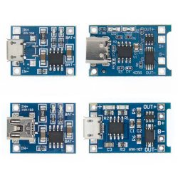 This is a linear charger IC – if you want 1 A out, you need 1 A in, and the input-output voltage difference multiplied by current is converted into heat. Thankfully, the TP4056 modules are built to handle high temperatures reasonably well, and you can add a heatsink if you want. Maximum charging current is set by a resistor between ground and one of the pins, default resistor being 1.2 kΩ resulting in 1 A current; for low-capacity cells, you can replace it with a 10 kΩ resistor to set a 130 mA limit, and you can find tables online for intermediate values.
There’s some cool things about the TP4056 IC that most people don’t know about if they’re using the modules as-is. The IC’s CE pin is hardwired to 5 V VIN, but if you lift that pin, you can use it to disable and enable charging with a logic level input from your MCU. You can monitor the charging current by connecting your MCU’s ADC to the PROG pin – the same pin used for the current setting resistor. There’s also a thermistor pin, typically wired to ground, but adaptable for a wide range of thermistors using a resistor divider, whether it’s the thermistor attached to your pouch cell or one you added externally to your 18650 holder.
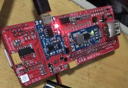 There’s problems with the TP4056 too – it’s a fairly simple IC. Efficiency isn’t an imperative where wall power is available, but the TP4056 does waste a decent bit of power as heat. A switching charger-based module avoids that, and often also lets you charge at higher currents if ever required. Connecting a cell in reverse kills the chip, and the protection circuit too – this mistake is easy to make, I’ve done that aplenty, and this is why you need spares. If you reverse the cell contacts, throw the board out – don’t charge your cells with a faulty IC.
Also, given the TP4056’s popularity, copies of this IC are manufactured by multiple different chip vendors in China, and I’ve observed that some of these copy ICs break more easily than others, for instance, no longer charging your cells – again, keep spares. The TP4056 also doesn’t provide charging timers like other, more modern ICs do – a subject we touched upon in the comment section of the first article.
All in all, these modules are powerful and fairly universal. It’s even safe to use them to charge 4.3 V cells, as due to the CC/CV operation, the cell simply won’t charge to its full capacity – prolonging your cell’s life as a side effect. When you need to go beyond such modules, there’s a myriad of ICs you can make use of – smaller linear chargers, switching chargers, chargers with built-in powerpath and/or DC-DC regulator features, and a trove of ICs that do LiIon charging as a side effect. The world of LiIon charger ICs is huge and there’s way more to it than the TP4056, but the TP4056 is a wonderful starting point.
The Protection Circuit You Will See Everywhere
Just like with charging ICs, there’s many designs out there, and there’s one you should know about – the DW01 and 8205A combination. It’s so ubiquitous that at least one of your store-bought devices likely contains it, and the TP4056 modules come with this combo too. The DW01 is an IC that monitors the voltage of your cell and the current going to and from it, and the 8205A is two N-FETs in a single package, helping with the actual “connect-disconnect the battery” part. There’s no additional current sensing resistor – instead, the DW01 monitors voltage across the 8205A junction. In other words, the same FETs used to cut the cell from the outside world in case of failure, are used as current sensing resistors. This design is cheap, prevalent, and works wonders.
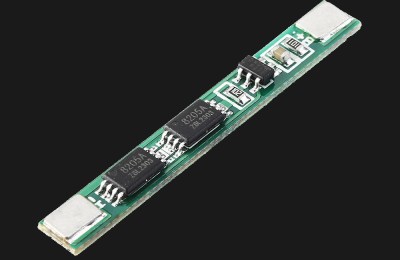 The DW01 protects from overcurrent, overdischarge and overcharge – the first two happen relatively often in hobby projects, and that last one’s handy if your charger ever goes rogue. If something wrong happens, it interrupts the connection between the cell’s negative terminal and GND of your circuit, in other words, it does low-side switching – for a simple reason, FETs that interrupt GND are cheaper and have lower resistance. We’ve also seen some hacks done with this chip – for instance, we’ve covered research from a hacker who figured out that the DW01 can be used as a soft power switch for your circuit – in a way that doesn’t compromise on safety. You only need to connect a GPIO pin of your MCU to the DW01, preferably through a diode – this comment describes an approach that seems pretty failure-resistant to me.
When you first connect a LiIon cell to the DW01+8205A combination, sometimes it will enable its output, but sometimes it won’t. For instance, if you have a holder for 18650s and a protection circuit connected to it, it’s a 50/50 chance that your circuit will power up once you insert the battery. The solution is simple – either connect a charger externally, or short-circuit the OUT- and B- with something metal (I often add an external button), but it’s annoying to deal with. Just like TP4056, the DW01+8205A combo dies if you connect the battery in reverse. Also, the DW01 is internally wired for 2.5 V overdischarge cutoff, which technically isn’t changeable. If you don’t have a separate software-controlled cutoff, the FS312 is a pin-compatible DW01 replacement with 3.0 V overdischarge point, helping you prolong your cell’s life.
You can buy a batch of ready-to-go protection circuit modules, or just use the protection circuit laid out on the TP4056 module PCB. You can also accumulate a decent stock of protection circuits by taking them out of single-cell batteries whenever the cell puffs up or dies – take caution not to puncture the cell while you do it, please.
All The Ways To Get 3.3 V
For a 4.2 V LiIon cell, the useful voltage range is 4.1 V to 3.0 V – a cell at 4.2 V quickly drops to 4.1 V when you draw power from it, and at 3.0 V or lower, the cell’s internal resistance typically rises quickly enough that you will no longer get much useful current out of your cell. If you want to get to 1.8 V or 2.5 V, that is not a problem, and if you want to get to 5 V, you’ll use a boost regulator of some sort. However, most of our chips still run at 3.3 V – let’s see what our options are here.
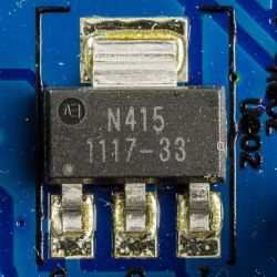
When it comes to LiIon range to 3.3 V regulation, linear regulators closely trail switching regulators in terms of efficiency, often have lower quiescent (no-load) current if you seek low-power operation, and lower noise if you want to do analog stuff. That said, your regular 1117 won’t do – it’s an old and inefficient design, and the 1117-33 starts grinding its gears at about 4.1 V. Instead, use pin-compatible, low dropout voltage replacements like AP2111, AP2114 and BL9110, or AP2112, MIC5219, MCP1700 and ME6211 if you’re okay with SOT23 stuff. All of these are linear regulators comfortable providing 3.3 V with input down to 3.5 V and sometimes even 3.4 V, if you’d like to power something like an ESP32. It’s hard to deny the simplicity of using a linear regulator – one chip and a few caps is all it takes.
If you want 500 mA to 1000mA or even more current on an ongoing basis, a switching regulator will be your best friend. My personal favourite is PAM2306 – this regulator is used on the Raspberry Pi Zero, it’s very cheap and accessible, and even has two separate output rails. Given its capability to do 100% duty cycle operation, it can extract a lot of juice out of your cells, often desirable for higher-power projects where runtime matters. And hey, if you got Pi Zero with a dead CPU, you won’t go wrong snipping a part of the PCB off and soldering some wires to it. When designing your own board, use datasheet recommendations for inductor parameters if the whole “picking the right inductor” business has you confused.
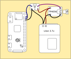 So, the PAM2306 is the regulator on the Pi Zero, and it’s also LiIon-friendly? Yep, you can power a Pi Zero directly from a LiIon battery, as all the onboard circuitry works down to 3.3 V on the “5 V” pins. I’ve tested it extensively in my own devices, and it even works with the Pi Zero 2 W. Combined with this powerpath and a charger, you have a complete “battery-powered Linux” package, with all the oomph that a Raspberry Pi provides – at cost of only a handful of components. One problem to watch out for is that MicroUSB port VBUS will have battery voltage – in other words, you’re best off filling the MicroUSB ports with hot glue just in case someone plugs a MicroUSB PSU there, and tapping the USB data testpoints for USB connectivity.
A Power Path To Join Them All
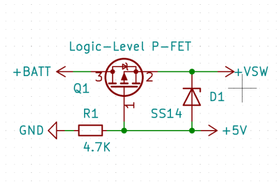 Now, you’ve got charging, and you got your 3.3 V. There’s one problem that I ought to remind you about – while you’re charging the battery, you can’t draw current from it, as the charger relies on current measurements to control charging; if you confuse the charger with an extra load, you risk overcharging the battery. Fortunately, since you have a charger plugged in, you must have 5 V accessible. It’d be cool if you could power your devices from that 5 V source when it’s present, and use the battery when it’s not! We typically use diodes for such power decisions, but that’d cause extra voltage drop and power losses when operating from the battery. Thankfully, there’s a simple three-component circuit that works way better.
In this power path circuit, a P-FET takes role of one of the diodes, with a resistor opening the FET while the charger’s not present. The P-FET doesn’t have a voltage drop, but instead has resistance in fractions of an ohm, so you avoid losses when the charger’s not plugged in. Once the charger is connected, the FET closes, and the charger powers your circuit through the diode instead. You need a logic-level P-FET – IRLML6401, CJ2305, DMG2301LK or HX2301A would fit, and there’s thousand others that will work. As for a diode, a default Schottky like 1N5819 (SS14 for SMD) will do. It’s a ubiquitous circuit and deserves its place in circuit toolboxes.
You can buy shields and modules that contain all of these parts and sometimes more, on a single board. You can also buy ICs that contain all or some of the parts of this circuit, often improved upon, and not worry about the specifics. These ICs tend to be more expensive, however, and way more subject to chip shortages than the individual component-based solution. Plus, when issues arise, understanding of inner workings helps a whole lot. Thus, it’s important that the basics are demystified for you, and you don’t feel forced into reusing powerbank boards next time you want to make a device of yours portable.
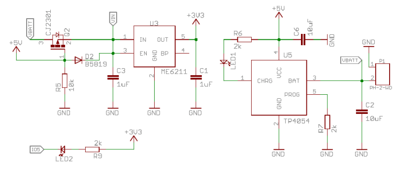
Be on the lookout on what other boards are doing. Often, you’ll see the charger + regulator + powerpath circuit described above, especially when it comes to cheaper boards with chips like the ESP32. Other times, you’ll see more involved power management solutions, like powerbank chips or PMICs. Sometimes they’re going to work way better than the simple circuit, sometimes it’s the opposite. For instance, some TTGO battery-powered boards use powerbank chips and overcomplicate the circuit, resulting in weird behaviour and malfunctions. A different TTGO board, on the other hand, uses a PMIC that’s way more suited for such boards, which results in flawless operation and even granular power management control for the user.
Hack Portable Devices Like You Couldn’t Before
Now you know what it takes to add a LiIon battery input connector to your project, and the secrets behind the boards that come with one already. It’s a feeling like no other, taking a microcontroller project with you on a walk as you test out a concept of yours. I hope I got you a bit closer to experiencing it.
Next time, I’d like to talk about batteries with multiple cells in series – BMSes, balancing and charging LiIon packs from different sources. That, however, will take a good amount of time for me to prepare, as I’d like to finish a few related projects first, and I recommend you check this coverage of ours out if you’d like to learn about that. In the meantime, I wish you luck in building your battery-powered projects!
0 Commentaires