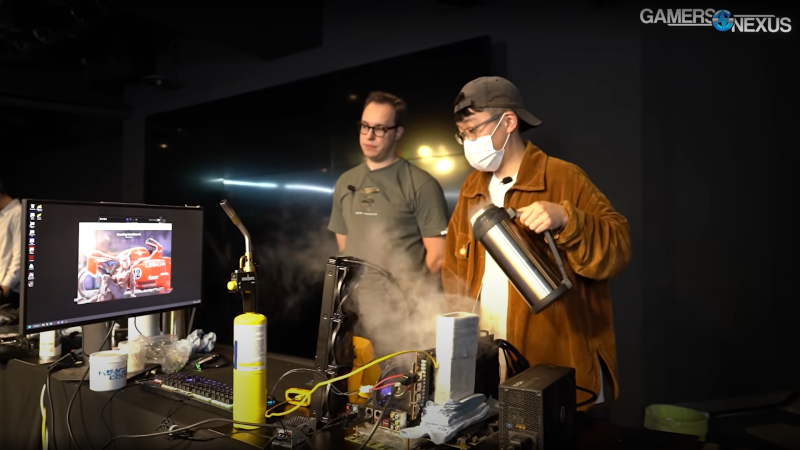
It’s not news that EVGA is getting out of the GPU card game, after a ‘little falling out’ with Nvidia. It’s sad news nonetheless, as this enthusiastic band of hardware hackers has a solid following in certain overclocking and custom PC circles. The Games Nexus gang decided to fly over to meet up with the EVGA team in Zhonghe, Taiwan, and follow them around a bit as they tried for one last overclocking record on the latest (unreleased, GTX4090-based) GPU card. As you will note early on in the video, things didn’t go smoothly, with their hand-lapped GPU burning out the PCB after a small setup error.
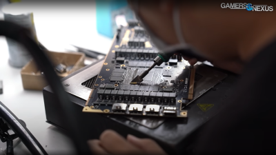
The fun parts of the video show some behind-the-scenes details of the EVGA GPU operation, including some sections of BGA reworking which are pretty informative (but we’d like more detail, thanks!) showing that even with only a handful of AD102 Silicon available and a few prototype PCBs, even letting out the magic smoke is not necessarily the end of the show.
But why hand-lap the die? Apparently, the surface is pre-curved outwards, so that when it warms up under load, the die surface ends up flat, making the best contact with the thermal interface surface of the cooler. But [biso biso] uses liquid nitrogen for their overclocking speed records, and that has the opposite effect, with the extreme cooling (about -90 Celsius) causing the die to flex differently, and ‘crack’ the thermal paste, ruining the thermal contact with the cooling media. Lapping the die back to flat, apparently reduces this problem.
On the rework side of things, (14:45 in the video) they needed to remove the lapped GPU from the blown card using a standard IR rework station. The technician waited for the moment all the GPU balls were molten, before quickly whipping away the smoking chip with a vacuum pickup. Next, it was thoroughly cleaned and brushed with flux whilst sitting on a preheater. After hand-tinning the pads, it’s ready for the re-balling jig, and given a sprinkling of fresh balls, before a trip through the oven to fix them in place. Finally, after ultrasonic cleaning, it was ready for testing on a socketed development card. Once a test pass was achieved, the GPU was mounted onto a suitably prepared donor PCB, likely using the same reflow station seen earlier (but that was not shown,) it’s a simple process, but a skilled one that the repair team does all the time, making it look effortless. We’d sure break a sweat trying to do this!
Think all this PC overclocking, just for a short-lived record is somewhat pointless? How about an overclocked TI-84 instead?
And, an earlier video with a tour of the EVGA shop:
Thanks to [Simon] for the tip!
0 Commentaires