
If you ever work with a circuit that controls a decent amount of current, you will often encounter a FET – a Field-Effect Transistor. Whether you want to control a couple of powerful LEDs, switch a USB device on and off, or drive a motor, somewhere in the picture, there’s usually a FET doing the heavy lifting. You might not be familiar with how a FET works, how to use one and what are the caveats – let’s go through the basics.
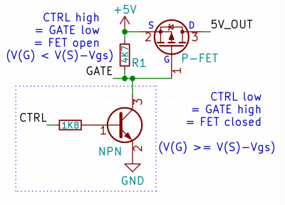 Here’s a simple FET circuit that lets you switch power to, say, a USB port, kind of like a valve that interrupts the current flow. This circuit uses a P-FET – to turn the power on, bring the GATE signal down to ground level, and to switch it off, bring it back up, where the resistor holds it by default. If you want to control it from a 3.3 V MCU that can’t handle the high-side voltage on its pins, you can add a NPN transistor section as shown – this inverts the logic, making it into a more intuitive “high=on, low=off”, and, you no longer risk a GPIO!
This circuit is called a high-side switch – it enables you to toggle power to a device at will through a FET. It’s the most popular usecase for a FET, and if you’re wondering more about high-side switches, I highly recommend this brilliant article by our own [Bil Herd], where he shows you high-side switch basics in a simple and clear way. For this article, you can use this schematic as a reference of how FETs are typically used in a circuit.
Small Talk
There’s different kinds of FETs – MOSFETs, JFETs, and a few dozen less popular but still abundant ones. When talking about a FET, people usually mean a MOSFET, and that’s what this article is going to talk about, too – other types aren’t as popular for the usual hacker purposes, and I don’t know much about JFETs to begin with. They’re all field-effect transistors, however, siblings to the other kind of transistor that’s abundant – BJTs (Bipolar Junction Transistor), popular enough that we typically just refer to them as NPN or PNP transistors. These are all under the transistor umbrella, but when people say “transistor”, they usually mean BJT, and when people say “FET”, they usually mean “MOSFET”.
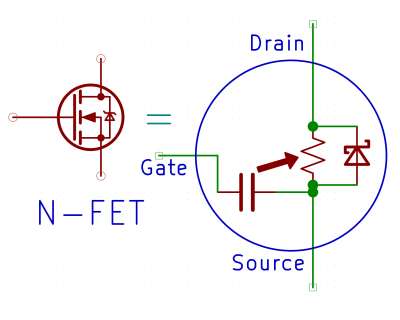 You can imagine a FET as a resistor you can control, and its resistance can go as low as a fraction of an ohm (open), or to an infinitely high resistance for the purpose of your design (closed). You open the FET by charging and discharging its gate – at its simplest, you can imagine the gate as a capacitor. To sum it up, a FET is a transistor that acts as a resistor, with a built-in capacitor for controlling the FET’s resistance.
This makes FETs uniquely wonderful for things like power rail switching! When controlling a device’s power rail with a BJT, a voltage drop of at least 0.3 V is inevitable due to the way BJTs work – wasting power into heat as a result, and a no-go for digital devices where supply voltage matters. A FET in the same application, however, will just be an inline sub-ohm resistance – efficient and friendly. This is the main reason why FETs are used for power switching applications, and you will see FETs in all kinds of places as a result.
Now, a FET doesn’t instantly go from “fully open” to “fully closed” – just like with BJTs we all know and love, there are in-between states too, where resistance is not as low as the FET goes, but also not infinite – the FET is partially open, or, in other words, in its linear region. You can reach the linear region by applying an almost-open-but-not-quite kind of voltage to the gate, and by taking advantage of this, you can build an amplifier, an electronic load, or a constant-current driver for some LEDs. For switching purposes, however, a FET in the linear region is something you want to avoid – high resistance means high losses and the need to dissipate that heat somehow.
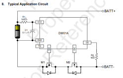 Due to the way that FETs are built, each FET has a diode built-in, known as a “body diode”. You can’t avoid this diode – it’s there to stay; you can only account for its existence when wiring things up. If a diode is undesirable, a way to avoid it is by putting two FETs back-to-back. This is how LiIon battery protection circuits work – they need to protect the battery from overdischarge by shutting off the current that flows out, but they also need to protect from overcharge by shutting off the current that flows in, and putting two FETs in series with the diodes facing each other is one way to accomplish that. If you look at a higher-current LiIon battery BMS, you will inevitably find two FETs wired up like that, or even two rows of FETs put in parallel!
How does a FET actually work on a physical level, without the simplifications? Here’s a video from [Thomas Schwenke] on FETs specifically, and also one from [EEVblog] that talks about both BJTs and FETs. There are also myriad learning material and examples online, like this beautiful GIF from Wikipedia. You don’t exactly need to know this, but it might help, and it’s absolutely fascinating, too!
Opening Up
To open a FET, you need to apply a voltage to the gate that exceeds the FET’s Vgs threshold and doesn’t exceed the Vgs(max) value. Both of these are found in the datasheet, of course. Beware – Vgs in the datasheet (and online retailer part pickers!) is often given for some acceptable value of resistance, but not for the lowest resistance that the FET can achieve, so, you’ll want to check the Vgs-to-resistance graph in the datasheet. Now, in Vgs, G stands for gate and S stands for source – the third pin is drain; once the FET opens, current flows from source to drain. Of course, the gate control voltage has to be supplied relative to source, too.
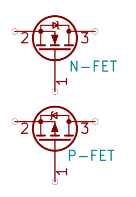 Just like with NPN and PNP transistors, there are N-FETs and P-FETs. N-FETs are like NPN transistors – the gate pin needs to have higher voltage than the source pin for the FET to open. P-FETs are like PNP transistors, too – the gate pin of a P-FET needs to have lower voltage than the source pin, of course, exceeding Vgs; in P-FET datasheets, Vgs is shown as a negative number, say, “-1.7 V”. As you might have noticed, it’s easiest to use P-FETs for high-side switching and N-FETs for low-side switching – as long as your Vgs is smaller than your power rail voltage, you don’t have to go outside of the range of voltages available within your circuit.
Now, when wiring a FET up, remember about the body diode – if you use a FET for load switching and wire it up the wrong way by mixing up source and drain, your device will always be powered through the body diode, no matter if the FET is open or not. On the other hand, checking with the datasheet for the pinout will eliminate this problem, and when drawing the schematic, the FET symbol will often have the diode drawn inside – or, at least, an arrow going from the same pin.
As for the naming, it’s easy to remember – when doing high-side switching with P-FETs or low-side switching with N-FETs, you connect your power source to the source pin, positive rail in case of a P-FET or the negative rail in case of an N-FET. Even if you need a FET for a different purpose, this particular mnemonic can remind you from which to which pin the body diode goes! P-FET, positive source. N-FET, negative source.
Once you got a FET, there’s a few ways to put it into a circuit. If you’re switching a 3.3 V power rail and your microcontroller is 3.3 V, you might as well drive the FET directly with a GPIO – while charging a FET’s gate isn’t always GPIO-friendly, gate capacitance won’t be much of a load on your GPIO at a small scale, so it’s a good shortcut in hacker projects; if concerned, you can add a series resistor between the gate and GPIO, say, 100 Ω. It’s also quite popular to drive low-side switching N-FETs with a GPIO, just like we do with NPN transistors!
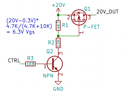
However, if your voltages don’t match, say, you’re controlling a 12 V load with a P-FET and a 3.3 V GPIO, there is another, way more popular way, that you’ve seen in our first example schematic – use another FET or BJT to pull the gate into one direction, and a resistor to pull it into another; if you need to keep your Vgs within a certain range, just add an extra resistor between the gate and the control transistor to form a voltage divider!
This is super useful, but not flawless. The gate is a capacitor, so charging or discharging it through a resistor will take more time than doing the opposite with a transistor, so the resistor-driven direction will spend more time in the linear region. This isn’t much of a problem for switching loads on and off occasionally, but it will bite you if you decide to do higher-frequency PWM – say, you’re driving LEDs or controlling speed of a motor, with the motor’s inductance messing things up even further. That’s where FET drivers come in – it’s a small chip that has a push-pull stage inside of it that helps you drive the gate strongly despite the capacitance, and keep Vgs within an acceptable range, too. More or less, connect your control GPIO to one side of the chip, your FET’s gate to another, follow the gate driver’s datasheet, and you’re golden.
Setting Boundaries
Of course, FETs have their limitations and nuances – there are myriad FETs in SOT23 packages that all look the same, but only some of them will keep up when you need to drive a few meters of an LED strip. The most important parameters are drain-source maximum current and voltage – these define the kind of load you can drive with a FET. If you want to drive a 12 V / 3 A load, it would be wise to pick a 20 V / 4 A Vds/Ids FETs, and if it’s a 3.3 V / 1 A, a 12 V / 3 A FET is the usual choice. Oh, and, the body diode might look extremely convenient, say, if you’re switching inductive loads, as it would dissipate some of the backwards EMF that the FET might get – don’t rely on it too much though, if you need a diode, adding an extra diode in parallel is a better way.
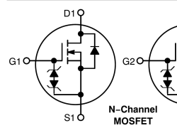
Have you found some nice and cheap FETs, or maybe you got some good ones in your stash, but they’re a bit short on the maximum current they can handle? Good news – you can often put similar FETs in parallel to increase the maximum current capacity! Unlike diodes, most FETs have a positive thermal coefficient – as more current flows through a FET and its temperature increases, its resistance increases too, which results in paralleled FETs balancing each other out – even if their parameters aren’t perfectly equal. You don’t even need to have separate driving circuits – just parallel FETs together, all three pins ganged, and it will work.
The gate pin is more touchy than the drain and source – for instance, it’s quite ESD-sensitive, and some FETs even have ESD protection diodes built in, wired between gate and source. Unlike with BJT transistors that need a constant current flow, you only need to charge a gate once for the FET to remain open for a fair bit – and it’s such a small amount of charge that you can often literally charge a FET’s gate by merely touching it with your finger, if the gate isn’t being actively pulled into any direction. See the R1 resistor in the intro circuit? It keeps the gate discharged and the FET closed unless it’s not actively being opened – without this resistor, the FET would not close on its own, and it would be susceptible to all sorts of noise. Unless you’re using a gate driver, you’ll absolutely want a gate-source resistor.
Also, generally, maximum Vgs threshold is way lower than Vds threshold – for instance, for a 30 V Vds FET, it’s not uncommon to see the maximum Vgs be 12 V or so; exceed it and the FET is quite likely to fail. Let’s say, you’re switching 20 V with such a P-FET, in the usual high-side switching configuration, and you get good Rds (drain-source resistance) at -6 V – you’ll want to keep the gate at about 12 V. Again, the easiest way to do that is a voltage divider, and the gate pull resistor will fit nicely into the picture!
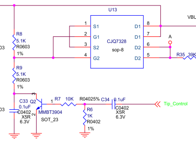 When a FET fails, it usually fails short-circuit – this is quite bad if you’re relying on the FET for anything critical, but if there is one upside, it’s that it is quite easy to debug when your FET has failed. Some products, like the Pinecil, use two FETs in series to further safeguard from such issues – indeed, having a soldering iron’s tip heat up uncontrollably is bad for your customers. Other products just use a single FET and don’t bother – failures are overall rare.
Speaking of the Pinecil, it uses an unorthodox driving circuit – it has an NPN transistor, but its base driven through a capacitor, so that only the AC component of the driving signal gets through. As a result, if the main MCU hangs and the control GPIO is stuck high, the FET won’t stay enabled!
Until Next Time
Would you like to learn more in-depth about FETs? There’s plenty of information online. For instance, this TI app note about driving FETs is wonderful. Over here at Hackaday, we’ve also taken a look at FETs in a few different contexts – CMOS logic, high voltage switching, part sourcing and general transistor wrangling, as well as covered a few introductory guides.
Of course, there’s way more fun things to learn about FETs! Next time, let’s move from schematic snippets to real-world uses – I want to show you a bunch of cool circuits that use FETs in perhaps less conventional ways; from reverse polarity protection to soft-start circuits and level-shifting, there’s a number of purposes that a FET could have on your board. Oh, and there will be part number recommendations, part picker tips, and some FET trivia that you might find useful for your hacking journeys and completing your FET mental map!
0 Commentaires