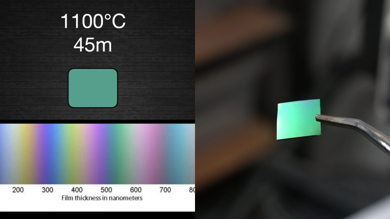
Doing anything that requires measurements in nanometers is pretty difficult, and seems like it would require some pretty sophisticated equipment. But when the task at hand is growing oxide layers on silicon chips in preparation for making your own integrated circuits, it turns out that the old Mark 1 eyeball is all you need.
Alert readers may recall that [ProjectsInFlight] teased this process in his previous video, which covered the design and construction of a DIY tube furnace. In case you missed that, a tube furnace is basically a long, fused quartz tube wrapped in electrical heating elements and lots of insulation, which is designed to reach the very high temperatures needed when making integrated circuits. The tube furnace proved itself up to the task by creating a thin layer of silicon dioxide on a scrap of silicon wafer.
In the current work, [ProjectsInFlight] takes that initial success and builds on it. A lot of the video below is devoted to explanations of what exactly a silicon oxide layer is and why you’d need one; if you’ve never been introduced to the subject matter or your understanding is shaky, this section is actually really valuable. The actual creation of silicon oxide starts at about the 7:45 mark, with an exploration of the effect of time in the furnace on layer thickness. This is measured by the color change on the surface of the silicon as the silicon oxide layer grows. It’s a bit subjective, but with some careful measurements of time and temperature, the results are pretty predictable.
One area where [ProjectsInFlight]’s simple tube furnace design caused problems was with maintaining a proper atmosphere. As he touched on in the first video, silicon oxide formation is much quicker if water vapor is present. He used a simple steam generator — a flask of water on a hot plate — but found that his oxides weren’t forming as expected because the steam was actually condensing before even making it into the tube furnace. The solution was simple — more heat and better insulation — and he was able to reliably build oxide layers in the 350 to 400 nm range.
This looks like great work, and we’re excited to see the next steps along [ProjectsInFlight]’s road to homebrew semiconductors.
0 Commentaires