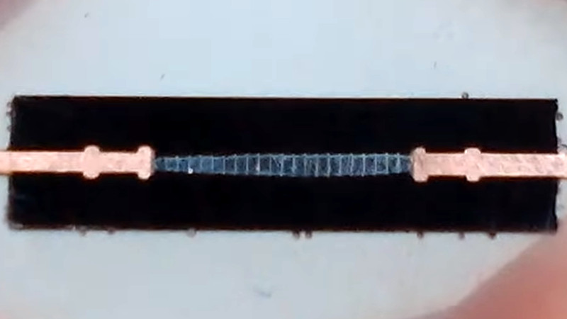
When we use an electronic component, we have some idea of what goes on inside it. We know that inside a transistor there’s a little piece of semiconductor with a junction made from differently doped regions etched into it, and in a capacitor, there will be metalized plates on the surface of some kind of dielectric. Reverse engineering has given us extensive die photography of integrated circuits, but there remain a few component mysteries to be uncovered. One is laid bare by [WizardTim], as he cross-sections a 20KV high-voltage diode.
A conventional low-voltage silicon diode has a forward voltage drop of about 0.7V and a relatively low maximum reverse voltage, for example with the 1N4001 rectifier it’s 50V. For the higher-spec 1N4007, the reverse voltage rating is 700V. This diode has a 25KV reverse voltage, and a clue to its construction comes in its quoted 45V forward voltage. Sure enough, when mounted in resin and carefully sanded and polished flat it reveals its interior as a stack of diodes in series to increase the reverse voltage at the expense of forward voltage.
Revealing the inner workings of an unusual component is fascinating, and the lapping technique used is definitely worth a look. It’s something we’ve seen before, for example in reducing CPU thickness for increased performance.
0 Commentaires