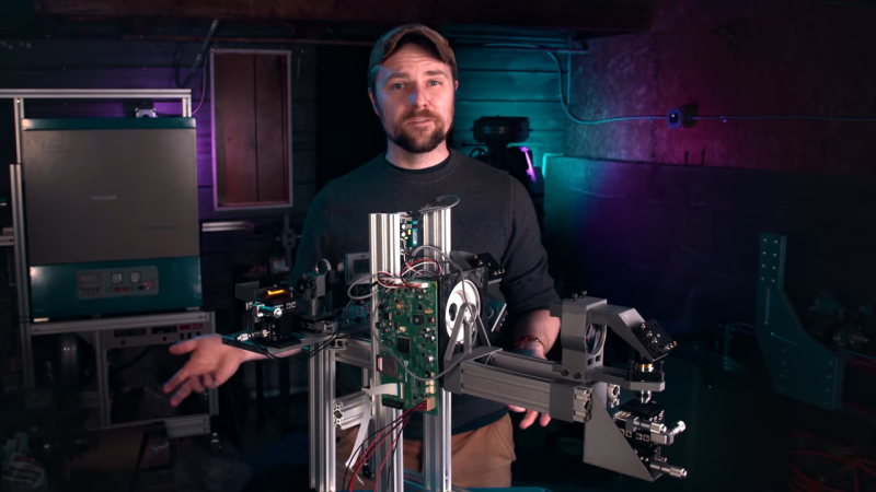
What does it take to make your own integrated circuits at home? It’s a question that relatively few intrepid hackers have tried to answer, and the answer is usually something along the lines of “a lot of second-hand equipment.” But it doesn’t all have to be cast-offs from a semiconductor fab, as [Zachary Tong] shows us with his homebrew direct laser lithography setup.
Most of us are familiar with masked photolithography thanks to the age-old process of making PCBs using photoresist — a copper-clad board is treated with a photopolymer, a mask containing the traces to be etched is applied, and the board is exposed to UV light, which selectively hardens the resist layer before etching. [Zach] explores a variation on that theme — maskless photolithography — as well as scaling it down considerably with this rig. An optical bench focuses and directs a UV laser into a galvanometer that was salvaged from an old laser printer. The galvo controls the position of the collimated laser beam very precisely before focusing it on a microscope that greatly narrows its field. The laser dances over the surface of a silicon wafer covered with photoresist, where it etches away the resist, making the silicon ready for etching and further processing.
Being made as it is from salvaged components, aluminum extrusion, and 3D-printed parts, [Zach]’s setup is far from optimal. But he was able to get some pretty impressive results, with features down to 7 microns. There’s plenty of room for optimization, of course, including better galvanometers and a less ad hoc optical setup, but we’re keen to see where this goes. [Zach] says one of his goals is homebrew microelectromechanical systems (MEMS), so we’re looking forward to that.
0 Commentaires