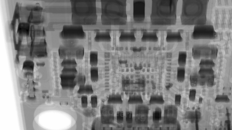
Most Hackaday readers will know to some extent what lies inside their computer, even if this is only at a block diagram level listing the peripherals. But what is physically on a modern computer board? [Jeff Geerling] has subjected a Raspberry Pi 5 to a medical imager, and shares with us the many layers of parts and PCB he found there. With a six-layer board and a heap of large BGA chips on it, there’s a lot to look at.
For readers who are used to working with printed circuit boards, it’s likely the techniques involved in the design will not be new. For us, the magic lies in the scale. The sheer number of interconnects on the board is impressive enough, but when it becomes possible to peer into the SoC package it becomes evident that there’s an internal PCB with some of the smallest vias we have ever seen. [Jeff] goes on to show us part by part around the board, on the way reminding us that some of the earliest Pi boards had to be reworked to replace Ethernet jacks without magnetics.
There’s a beauty to these ghostly images which might not be apparent to anyone who hasn’t stared obsessively at a PCB in a CAD package while it takes shape. The images show the work of the PCB designer’s art at a fine scale. We’d almost go as far as to suggest they be viewed as fine art instead of industrial design. Take a look, the video is below the break.
If this art is a bit big for you, then look at ASIC design – which takes things down to the microscopic level of the doped silicon structures within these amazing chips.
0 Commentaires